Co-Packaged Optics (CPO): Evaluating Different Packaging Technologies
2024年8月22天
Dr Yu-Han Chang

The rise of co-packaged optics (CPO) is transforming modern data centers and high-performance networks by addressing critical challenges such as bandwidth density, energy efficiency, and scalability. CPO enhances interconnect bandwidth and energy efficiency by integrating optics and electronics within a single package, significantly shortening electrical link lengths. This innovation is crucial as data center traffic surges, driven especially by AI and high-performance computing. Unlike traditional pluggable optics, which struggle with power efficiency at higher data rates, CPO offers significant power savings, with early implementations showing 30-50% reductions in consumption. The integration of optics with silicon, enabled by advancements in chiplet-based technology and 3D-IC packaging, also reduces signal degradation and power loss. As data rates push beyond 800G and 1.6T, CPO provides a scalable path to future network demands. With growing industry support and exploration into AI applications, CPO is expected to revolutionize network infrastructure with higher efficiency and capacity.
The role of heterogeneous integration for CPO
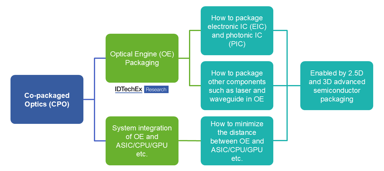
Heterogeneous integration is key to co-packaged optics (CPO), enabling the integration of the optical engine (OE)—which includes photonic ICs (PICs) and electronic ICs (EICs)— with switch ASICs or XPUs on a single package substrate. The packaging approaches for CPO are generally categorized into two types: one involves the packaging of the optical engine itself, and the other focuses on the system-level integration of the optical engine with ICs like ASICs or XPUs. Both approaches require the use of advanced 2.5D and 3D semiconductor packaging techniques. IDTechEx's latest report, "Co-Packaged Optics (CPO) 2025-2035: Technologies, Market, and Forecasts", delves into how various packaging technologies facilitate the heterogeneous integration of CPO. The report offers in-depth insights, including technology benchmarks, a range of case studies, a roadmap and outlook for the future, and a market forecast for CPO, segmented by different packaging technologies. In this article, IDTechEx will highlight key findings from its report on the integration of EICs and PICs.

Overview of CPO packaging approaches. Source: IDTechEx
Integration options for EIC/PIC

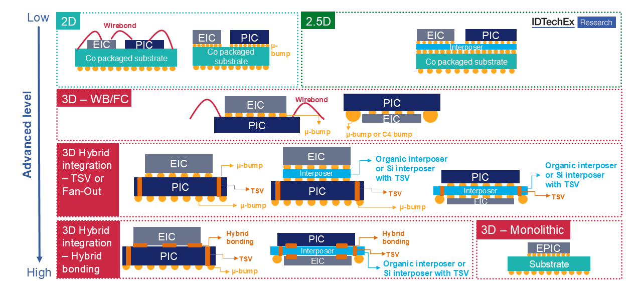
2D to 3D EIC/PIC Integration Options. Source: IDTechEx
Integrating photonic and electronic components can be accomplished through several methods, each offering distinct benefits and facing particular challenges.
2D Integration involves placing the PIC and EIC side by side on a printed circuit board (PCB), with connections made through wire bonds or flip-chip technology. The benefits of this method are the ease of packaging technologies, low complexity, and cost-effectiveness. However, the drawbacks include significant parasitic inductance, which leads to signal integrity issues and high energy consumption. Additionally, the overall I/O capabilities are restructured due to its pitch limitations and reliance on single-edge connections. Overall, while 2D integration is relatively easy to package, the use of wire bonds limits transceiver bandwidth and increases energy consumption, making it less suitable for high-performance applications.
2.5D Integration presents a middle ground by mounting both the EIC and PIC onto a passive interposer equipped with through-silicon vias (TSVs). This method reduces packaging parasitics between the EIC and PIC by using microbumps or copper pillars, which facilitate higher I/O connections and enable finer routing for increased bandwidth. Additionally, the use of interposers allows for the incorporation of waveguide layers, which can enhance optical signal redistribution and support better signal integrity. However, this approach comes with its own set of challenges. The development and fabrication costs for 2.5D integration are higher compared to 2D integration. Additionally, while it improves on 2D integration, 2.5D integration still exhibits higher parasitics than 3D integration, which impacts overall performance.
3D Hybrid Integration takes a more advanced approach by stacking the EIC on top of the PIC using advanced semiconductor packaging techniques such as Through-Silicon Via (TSV), high-density fan-out, Cu-Cu hybrid bonding, or an active photonic interposer (using PICs as an interposer as shown in the figure). Generally, a 3D integration approach significantly reduces parasitics and supports dense pitch configurations, enhancing performance. However, managing heat dissipation is a challenge, as the heat from the EIC can affect the PIC, requiring advanced thermal management solutions.
Among those different packaging approaches, Through-Silicon Via (TSV) technology is considered one of the critical technologies for integrating EIC and PIC due to its benefits in power delivery and communication efficiency. TSVs minimize IR drop and inductance, providing reliable power to critical components while enabling shorter interconnects for improved communication. Despite signal integrity challenges at high frequencies due to silicon's dielectric properties, TSVs' smoother metal surfaces help mitigate the skin effect, making them ideal for advanced EIC/PIC integration. According to Cisco, their 3rd generation of optical engine uses 3D TSV (Through-Silicon Via) advanced packaging technology. The use of TSV addresses power integrity bottlenecks caused by the challenges of delivering power efficiently to active devices on the PIC operating at high frequencies and the increasing number of active devices in the EIC.
3D Cu-Cu hybrid bonding technology, which supports bump pitches in the single-digit micrometer range, is emerging as a key solution for minimizing parasitics at the EIC/PIC interface. This technology, already used in high-end processors, offers significant advantages by reducing parasitics, which leads to lower power consumption and enhanced performance. TSMC is advancing this approach through its SoIC technology, branded as COUPE, for stacking EIC and PIC, aiming to leverage hybrid bonding to achieve superior integration efficiency and performance.
3D Monolithic Integration, the most advanced and still under development, involves embedding photonic components within an existing electronic process node with minimal changes. This approach integrates active photonics and electronics within the same die, reducing parasitics and simplifying packaging by eliminating the need for interface pads and bumps. However, it often relies on older CMOS process nodes, which can lead to suboptimal photonic performance and higher energy consumption. Despite these limitations, 3D monolithic integration offers reduced impedance mismatch and simplified packaging.
As co-packaged optics (CPO) becomes a pivotal solution for high-end data centers, the choice of packaging technology remains under active debate and research. Each integration method presents unique benefits and challenges, and it's crucial to consider not just the packaging of the optical engine but also the comprehensive system integration involving the co-design of ICs (switch ASICs/XPUs) and optical engines. IDTechEx's latest report, "Co-Packaged Optics (CPO) 2025-2035: Technologies, Market, and Forecasts", explores various packaging technologies that enable the heterogeneous integration of CPO, including optical engine integration and system-level packaging. The report provides detailed insights, including technology benchmarks, case studies, future roadmaps, and market forecasts segmented by different packaging technologies.
For more information on this IDTechEx report, including downloadable sample pages, please visit www.IDTechEx.com/CPO.
For the full portfolio of related research available from IDTechEx, please see www.IDTechEx.com/Research/Semiconductors.
About IDTechEx
IDTechEx provides trusted independent research on emerging technologies and their markets. Since 1999, we have been helping our clients to understand new technologies, their supply chains, market requirements, opportunities and forecasts. For more information, contact research@IDTechEx.com or visit www.IDTechEx.com.