
End User Needs. New Innovations. Big Brands.
November 18-19, 2015 | Santa Clara, CA, USA
Tours
This event will take advantage of being located in Santa Clara and the Bay Area - a center of excellence for these technologies - by hosting tours to some of the leading organizations working on this technology in this region.
Places on these tours are limited and are offered to attendees of the masterclasses first. You can only attend one tour per day.
How to apply
For more information and to book your place on the company tours, please email: Corinne Jennings at c.jennings@IDTechEx.com
Apply for tour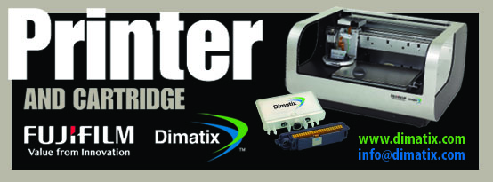
FUJIFILM Dimatix
Tour is fully booked

The FUJIFILM Dimatix tour provides an overview of the company, its products and its people with a walk-through of its manufacturing facility.
FUJIFILM Dimatix, Inc. is the world's premier provider of piezoelectric inkjet printheads and systems. As of July 2006, FUJIFILM Dimatix is a wholly owned subsidiary of FUJIFILM Corporation. FUJIFILM Dimatix has more than 29 years experience in advancing the performance of drop-on-demand dispensing devices and applications, and its state-of-the-art technology provides solutions for the printed electronics industry.
FUJIFILM Dimatix's MEMS-based technology lets inkjet printing create products like displays and electronics, RFID antennas, smart tags, DNA arrays, smart packaging and wearable electronics. The Dimatix Materials Printer DMP-2831 is a low-cost, cartridge-based piezo inkjet printing system that enables direct deposition of functional fluids - including nanoparticle-based metallic and organic materials.
Tuesday, November 17 / 12.00 noon - 2.15pm
During the break between the morning and afternoon masterclasses.
We will be meeting at 11.50 am in the Main Lobby, Santa Clara Convention Center
Stanford University

Stanford University is located between San Francisco and San Jose in the heart of Silicon Valley, and is recognized as one of the world's leading research and teaching institutions. Almost 7,000 undergraduates and 8,000 graduate students are engaged in studies over roughly 60 majors and myriads of research projects.
The tour to Stanford University will involve a visit to the SNF, SNSF and Electrical Engineering, Computer Science, and Material Science and Engineering buildings.
https://snsf.stanford.edu
http://snf.stanford.edu
Friday, November 20 / 12.00 noon - 2.15pm
During the break between the morning and afternoon masterclasses.
We will be meeting at 11.50am at the Main Foyer, Second Floor/200 Rooms of the Santa Clara Convention Center.

Kateeva
Tour is fully booked

This year, visitors will tour Kateeva's new Global Headquarters in Newark. With more than twice the square footage of its previous facility in Menlo Park, the new facility combines business, development and manufacturing operations in one location. You can find details here.
The tour will begin with a brief overview of the latest innovation happening at Kateeva. From there, visitors will view 3 core components of Kateeva's operations, outlined below. They'll depart with a good snapshot of the business of making an inkjet printing manufacturing equipment solution for OLED mass-production.
Tour highlights
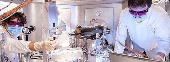
- Window tour of OLED cleanroom and R+D printing laboratory. The primary purpose of the OLED cleanroom is to finish devices in which the charge transport and emitting layers are deposited by ink jet printing. This facility includes vacuum deposition tools, as well as spin coating and characterization tools. The R+D laboratory contains multiple R+D tools manufactured by Kateeva for OLED process development. Details of the tool capabilities will be discussed during the tour.
- Chemistry laboratory. Kateeva formulates OLED inks at its HQ. A brief description of Kateeva capabilities will be described.
- Window tour of demo tool facility, including G8-scale (2.2 m x 2.5 m substrate) manufacturing tool. A basic description of this manufacturing tool will be given, and capabilities highlighted.
Tuesday, November 17 / 12.00 noon - 2.15pm
During the break between the morning and afternoon masterclasses.
We will be meeting at 11.50 am in the Main Lobby, Santa Clara Convention Center

DuPont
Tour is fully booked

On the tour you will be taken to the Sunnyvale Technology Center, a global photovoltaic research center where DuPont will share their broader vision and latest developments in the realm of printed electronics.
www.mcm.dupont.com
Friday, November 20 / 12.00 noon - 2.15pm
During the break between the morning and afternoon masterclasses.
We will be meeting at 11.50am at the Main Foyer, Second Floor/200 Rooms of the Santa Clara Convention Center.