Tendances en matière de matériaux et de traitement pour les emballages de semi-conducteurs 2.5D et 3D

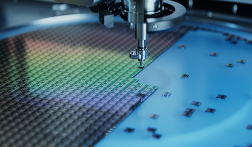
Advanced semiconductor packaging is designed to address the needs of high-bandwidth computing in today's data-centric world. The evolution of semiconductor packaging technologies has led to significant progress, transitioning from PCB board-level integration to more advanced wafer-level integration techniques like 2.5D and 3D packaging. These advanced packaging methods offer several benefits, including enhanced connection density, smaller physical footprints, and improved bandwidth, ultimately resulting in higher overall performance compared to traditional approaches.
To achieve these advancements, the selection of appropriate dielectric materials and the utilization of effective processing techniques are crucial. These factors directly contribute to achieving higher wiring density and bit rate per I/O, thereby impacting the overall bandwidth in semiconductor packaging. By carefully choosing dielectric materials with desirable properties and employing optimized processing techniques, semiconductor packages can deliver faster and more efficient data transfer.
In this webinar, Dr. Yu-Han Chang will present the latest research from IDTechEx's new report "Materials and Processing for Advanced Semiconductor Packaging 2024-2034", and will discuss:
- An overview of advanced semiconductor packaging technology: landscape and development
- Manufacturing methods and dielectric materials choice for 2.5D packaging
- A review of 3D Cu-Cu bonding packaging technology: materials and manufacturing processes barriers and future trend
Presenter
Video
Report
Related research
Reports
- Sensor Market 2026-2036: Technologies, Trends, Players, Forecasts
- Silicon Photonics and Photonic Integrated Circuits 2026-2036: Technologies, Markets, and Forecasts
- Critical Material Recovery 2026-2046: Technologies, Markets, Players
- Software-Defined Vehicles, Connected Cars, and AI in Cars 2026-2036: Markets, Trends, and Forecasts
