เส้นทางสู่รูปแบบเซมิคอนดักเตอร์ที่เป็นมิคอนดักเตอร์ที่เป็นมิตร
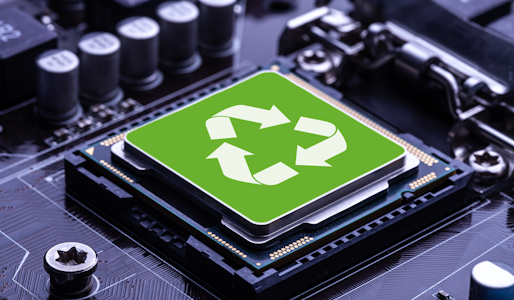
Electronics manufacturing requires vast amounts of energy, water, materials, and chemicals. With new legislation and ambitious emission reduction targets for manufacturers, adopting more sustainable processes and materials is essential. Semiconductor wafer patterning is a wasteful subtractive process, with photolithography and etching steps the largest contributors to emissions from integrated circuit manufacturing. This is exacerbated by advancing technology nodes. Significant improvements can be achieved through process optimization and advancements, improved abatement, and research into greener chemicals.
In this webinar, IDTechEx Technology Analyst Thomas Bithell will discuss:
- The issues with conventional semiconductor manufacturing and circuit patterning.
- Barriers and opportunities for sustainable manufacturing processes.
- The search for green chemicals and PFAS alternatives for semiconductor circuit patterning.
- The impact of EUV lithography on sustainability.
- Research focuses and advancements in dry etching.
This webinar shares some of the research from the new IDTechEx report, "Sustainable Electronics and Semiconductor Manufacturing 2025-2035: Players, Markets, Forecasts".
Presenter

Video
Report
Related research
Reports
- Nuclear Small Modular Reactors (SMRs) Market 2026-2046: Technologies, Players, Benchmarking, Forecasts
- Critical Material Recovery 2026-2046: Technologies, Markets, Players
- Materials Informatics 2025-2035: Markets, Strategies, Players
- Sustainable Electronics and Semiconductor Manufacturing 2025-2035: Players, Markets, Forecasts