Next-Generation RDL Materials in Advanced Semiconductor Packaging
Aug 11, 2023
Dr Yu-Han Chang
With the ever-increasing demand for higher performance and efficiency in electronic devices, the semiconductor industry is constantly pushing the boundaries of packaging technology. In the context of interconnected dies on a package, the system's performance relies heavily on the signaling that happens within the package. Two key metrics, bandwidth and power efficiency, play a pivotal role in determining the success of these advanced semiconductor packaging solutions. In this article, we will focus on the materials requirement for achieving higher bandwidth, one of the essential factors for improved communication between dies.
Bandwidth is a critical performance metric in advanced semiconductor packaging. It refers to the amount of data that can be transmitted or communicated between the dies on the package. Higher bandwidth allows faster and more efficient communication, enabling devices to process data at incredible speeds. Two primary factors are considered to measure bandwidth: IO/mm and Datarate/IO. IO/mm represents the density of I/O connections available on the die edge, while Datarate/IO refers to the data transfer rate of each I/O terminal measured in bps. By multiplying IO/mm by Datarate/IO, we calculate the bandwidth per millimeter of the die edge, which represents the total data that can be transmitted between dies. In simpler terms, bandwidth density indicates the number of bits transmitted and received between dies per mm (for 2D) or per mm2 (for 3D packaging).
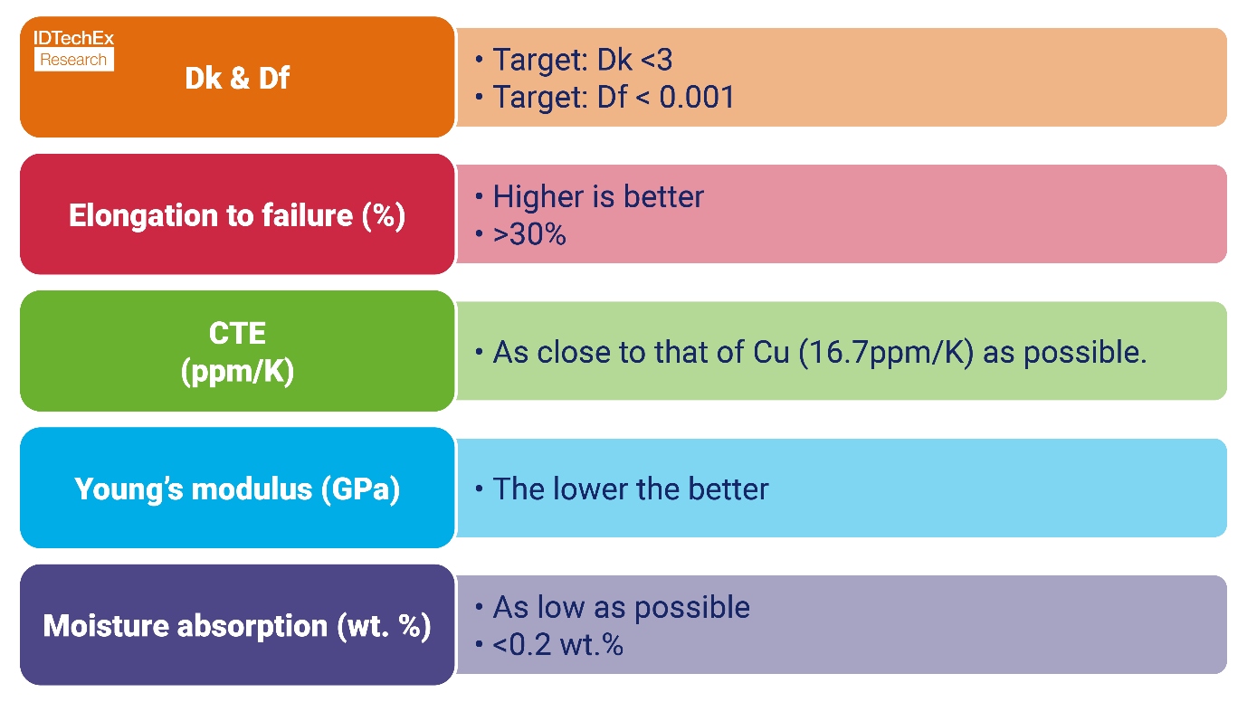
The performance of IO/mm and Datarate/IO heavily relies on the redistribution layer (RDL) within the package. Essential features of the RDL, such as Line/Space (L/S), via, and pad dimensions, play a crucial role in achieving optimal performance and data transmission within the package. The dielectric constant of materials used in the redistribution layer (RDL) directly impacts the datarate/IO. Currently, the finest L/S of RDL can be attained using inorganic dielectrics like SiO2, but the material's relatively high dielectric constant (Dk=3.9) makes it unsuitable for high-speed communication. Additionally, the process is also challenging and costly. As a result, researchers are actively exploring alternative dielectric materials, particularly organic options, which offer the advantages of lower dielectric constants and reduced costs. When selecting organic dielectric materials, several key parameters must be considered to ensure their suitability for the packaging process. IDTechEx's "Materials and Processing for Advanced Semiconductor Packaging 2024-2034" report identifies five key parameters crucial for organic dielectrics used in advanced semiconductor packaging.

Five key parameters for organic dielectric RDL. Source: IDTechEx - "Materials and Processing for Advanced Semiconductor Packaging 2024-2034"
Dk (Dielectric Constant) and Df (Loss Tangent):
A material's dielectric constant (Dk) determines its ability to support higher data rates without compromising signal integrity. Materials with low Dk are preferred for advanced semiconductor packaging as they reduce wire capacitance and allow for shorter interconnects between dies. Low-loss characteristics also minimize transmission loss in high-frequency communication devices, further enhancing bandwidth.
Elongation to Failure:
For multi-layer RDL (Redistribution Layer) with a higher copper coverage on each layer, a higher elongation to failure is favorable. This property ensures the material can withstand the stresses and strains associated with the packaging process and device operation without mechanical failure.
CTE (Coefficient of Thermal Expansion):
To ensure package reliability, the dielectric material should have a CTE similar to that of the copper metal layer. However, achieving this is challenging due to the inability to use filler particles that increase the dielectric permittivity of the polymer. SiO2 fillers, commonly used in polymer dielectrics, do not aid in reducing the Dk value as they need to be loaded in high volume. Additionally, the presence of fillers hinders the scaling of microvias, which are essential for advanced packaging technologies.
Young's Modulus:
For a reliable microvia design with a diameter of less than 5 µm, utilizing a polymer material with a low Young's modulus is crucial. A low modulus helps minimize the stress exerted on the copper, leading to enhanced overall package reliability.
Moisture Absorption:
Moisture absorption of the polymer material is crucial for long-term system reliability. High moisture absorption can lead to delamination and negatively impact both mechanical and electrical performance.
In conclusion, as technology continues to advance, the demand for even higher bandwidth and power efficiency in advanced semiconductor packaging will persist. Organic dielectrics have garnered significant interest due to their potential in offering low dielectric constant (Dk) characteristics, enhanced defect tolerance, and cost-effectiveness. However, it is crucial to acknowledge that selecting the appropriate material always involves trade-offs. For instance, while low dielectric constant polymers offer advantages, they may come with a higher coefficient of thermal expansion (CTE), which can adversely affect device reliability and packaging architectures. Therefore, it becomes imperative to carefully consider and adhere to the five key features and their requirements to ensure the successful development of advanced semiconductor packaging solutions.
IDTechEx's "Materials and Processing for Advanced Semiconductor Packaging 2024-2034" report offers a structured approach to understanding advanced semiconductor packaging. The report is divided into four main parts. The first part provides a comprehensive introduction to technologies, development trends, key applications, and the ecosystem of advanced semiconductor packaging. The second part focuses on 2.5D packaging processes, including dielectric materials, RDL fabrication techniques, and material selection for EMC and MUF. The third part delves into the innovative Cu-Cu hybrid bonding technology for 3D die stacking, offering insights into the manufacturing process and material selection. The report also includes a 10-year market forecast for the Organic Dielectric Advanced Semiconductor Packaging Module, providing valuable perspectives on market growth and trends for the coming decade.
To find out more about this IDTechEx report, including downloadable sample pages, please visit www.IDTechEx.com/MatsforASP.
IDTechEx's market research is differentiated through the primary information gathered, technical depth, and unbiased appraisals. IDTechEx covers a wide range of topics and helps understand the industry's pain points and unmet needs. For more information, please visit www.IDTechEx.com/research or contact research@IDTechEx.com.