This report has been updated. Click here to view latest edition.
If you have previously purchased the archived report below then please use the download links on the right to download the files.
Printed and Thin Film Transistors and Memory 2011-2021
| EXECUTIVE SUMMARY AND CONCLUSIONS | |
| 1. | INTRODUCTION |
| 1.1. | Importance of printed and potentially printed electronics |
| 1.1. | Growth in sales of silicon chips by value compared with growth in sales of printed and thin film electronic components. |
| 1.1. | Envisaged benefits of TFTCs in RFID and other low-cost applications when compared with envisaged silicon chips |
| 1.1.2. | Awesome new capability creates new markets |
| 1.1.3. | This is the new printing before it is the new electronics |
| 1.1.4. | Importance of flexibility, light weight and low cost |
| 1.1.5. | Creating radically new products |
| 1.1.6. | Improving existing products |
| 1.2. | How printed electronics is being applied |
| 1.2. | Typical carrier mobility in different potential TFTC semiconductors (actual and envisaged) |
| 1.2. | Examples of the radically new capabilities of printed electronics. |
| 1.3. | Types of early win and longer term project involving printed electronics 1995-2025 |
| 1.3. | Properties of the Polyera/ BASF n type printing ink for organic field effect transistors consisting of N,N Dioctyl-dicyanoperylene-3,4:9,10-bis(dicarboxyamide), PD18-CN2 |
| 1.3. | Importance of printed and thin film transistors and memory |
| 1.3.1. | Vision for the future |
| 1.3.2. | Benefits of thin film transistors and memory |
| 1.4. | Transistor basics and value chain |
| 1.4. | Logic circuits printed by PolyIC in Germany using a reel to reel process |
| 1.4.1. | How a transistor works |
| 1.4.2. | TFTC value chain |
| 1.5. | Transistor geometry and parameters |
| 1.5. | How printed electronics is being applied to products |
| 1.5.1. | Conventional geometry - horizontal transistors |
| 1.5.2. | New vertical geometry - vertical VFETs |
| 1.5.3. | New geometry - single layer transistors Plastic E Print |
| 1.5.4. | On off ratio and leakage current |
| 1.5.5. | Frequency, carrier mobility and channel length |
| 1.6. | Choice of materials for these transistors |
| 1.6. | Printed Electronics Applications |
| 1.6.1. | The thin film transistors on the back of today's LCD TV - a dead end? |
| 1.6.2. | Organic vs inorganic materials |
| 1.7. | Choice of semiconductor |
| 1.7. | Plastic film scanner |
| 1.7.2. | Organic semiconductors |
| 1.7.3. | Crystalline Silicon is a dead end? |
| 1.7.4. | Compound inorganic semiconductors |
| 1.7.5. | Breakthrough in printed inorganic performance in from Kovio |
| 1.7.6. | CMOS and the n type difficulty |
| 1.7.7. | Ambipolar semiconductors |
| 1.7.8. | Carbon nanotubes as thin film semiconductors |
| 1.7.9. | Importance of the dielectric layer |
| 1.7.10. | Importance of codeposition |
| 1.7.11. | Memory basics and value chain |
| 1.8. | Substrates |
| 1.8. | The value chain for manufacturing of printed electronics |
| 1.8.1. | High temperature and protective substrates vs low cost flexible |
| 1.8.2. | Polymers |
| 1.8.3. | Paper |
| 1.9. | Printing processes |
| 1.9. | Value chain for TFTCs and examples of migration of activity for players |
| 1.9.1. | Requirements |
| 1.9.2. | Ink jet vs fast reel to reel printing |
| 1.9.3. | Transfer printing of single crystals |
| 1.9.4. | 3D printed silicon transistors, Japan |
| 1.10. | Traditional geometry for a field effect transistor |
| 1.11. | Vertical organic field effect transistor VOFET showing a short channel length and a large cross section for current flow. The substrate is shown at the bottom. |
| 1.12. | ORFID view of the problems of the traditional horizontal transistor |
| 1.13. | Examples of vertical transistors |
| 1.14. | ORFID VOFET approach |
| 1.15. | The Plastic E print process |
| 1.16. | Structure of SSD diode and device operation |
| 1.17. | Principle of self aligned printing by Plastic Logic |
| 1.18. | Prevalence of organic vs inorganic materials in printed and thin film electronics today |
| 1.19. | PEDOT:PSS |
| 1.20. | Motorola summary of thin film FET issues concerning the dielectric layer . |
| 1.21. | Motorola view of available gate materials |
| 1.22. | The simple capacitor like structure for many printed devices including memory |
| 1.23. | Choices of substrate for printed electronics |
| 1.24. | Change in stiffness of PET vs PEN substrate material with temperature. |
| 1.25. | Biaxially oriented crystalline film |
| 1.26. | Factors influencing film choice- property set |
| 1.27. | Some candidate materials for flexible substrates |
| 1.28. | Requirements in printing thin film transistors |
| 1.29. | The big picture for printing transistors and memory in ever increasing numbers |
| 1.30. | Reel to reel printing of transistors and complete RFID labels by Poly IC |
| 1.31. | Options for high speed, low-cost printing of TFTCs |
| 1.32. | Choice of printing technology for silver RFID antennas today, where Omron and Avery Dennison use gravure despite volumes being no more than hundreds of millions. |
| 1.33. | Performance improvement in thermal ink jet over the years. |
| 1.34. | Benefits of ink jet printing of electronics |
| 1.35. | Thermal ink jet printed transistor evolution |
| 1.36. | Hybrid process improves performance |
| 1.37. | Transfer printed GaAs FETs on PET |
| 1.38. | Semprius opportunity space |
| 1.39. | Seiko Epson 3D printed silicon transistor |
| 2. | ORGANIC TRANSISTORS AND MEMORY - DEVELOPMENTS |
| 2.1. | History and prospective benefits |
| 2.1. | 64-bit organic transponder chip based on dual-gate thin-film-transistor technology, achieving 4.3kb/s data rate. |
| 2.1. | Printable polymer transistor dielectric PE-DI-1900 from BASF and Polyera |
| 2.2. | Holst Centre's 128 bit RFID transponder on plastic film. |
| 2.2. | RFID labels at Holst Centre |
| 2.3. | RFID labels from Poly IC |
| 2.3. | ACREO technology platform |
| 2.4. | Components of the ACREO low functionality approach to transistors |
| 2.4. | Lowest performance, lowest cost - ACREO |
| 2.5. | Organic dielectrics and ferroelectrics |
| 2.5. | ACREO electrochemical transistors |
| 2.6. | Electrochemical components electrical effects |
| 2.6. | High permittivity organic transistor gates by ionic drift |
| 2.7. | ACREO electrochemical transistors |
| 2.8. | ACREO objectives for electrochemical transistor circuits |
| 2.9. | ACREO electrochemical timer transistor |
| 2.10. | ACREO matrix addressed display. |
| 2.11. | Interactive games printed on paper |
| 2.12. | Concept demonstrator integrating printed electrochemical components and its patented "Dry Phase Patterning" of metal conductors. |
| 2.13. | ACREO applicational ideas |
| 2.14. | Transistor structure used |
| 2.15. | Ion modulation |
| 3. | INORGANIC COMPOUND TRANSISTORS - DEVELOPMENTS |
| 3.1. | History and summary of potential benefits |
| 3.1. | Early Hewlett Packard work on ink jet printing of inorganic compound semiconductors |
| 3.1. | A summary of the promised benefits of polymer ink used in pilot production of organic transistors vs two thin film inorganic semiconductors for transistors vs nanosilicon ink |
| 3.2. | Some properties of new thin film dielectrics |
| 3.2. | Printed flexible inorganic semiconductor |
| 3.2. | Semiconductors |
| 3.2.1. | Zinc oxide based transistor semiconductors |
| 3.2.2. | Amorphous InGaZnO |
| 3.2.3. | Progress towards p-type metal oxide semiconductors |
| 3.2.4. | Transfer printing silicon, GaN and GaAs on film |
| 3.2.5. | Tin disulphide |
| 3.3. | Inorganic dielectrics in devices |
| 3.3. | Transparent transistor |
| 3.3. | Benefits and challenges of R2R |
| 3.3.1. | Solution processed barium titanate nanocomposite |
| 3.3.2. | Hafnium oxide and HafSOx |
| 3.3.3. | Hybrid inorganic dielectrics - zirconia |
| 3.3.4. | Aluminium, lanthanum, tantalum and other oxides |
| 3.3.5. | Arizona State University's Flexible Display Center (FDC) and the University of Texas at Dallas |
| 3.4. | Chromium based technology |
| 3.4. | Imprint lithography |
| 3.4. | Material choices for transparent transistors |
| 3.4.1. | Printed oxide transistors at Oregon State University |
| 3.5. | Silicon nanoparticle ink |
| 3.5. | Amorphous thin film inorganic dielectric |
| 3.5.1. | Kovio |
| 3.6. | Printing aSi reel to reel |
| 3.6. | Example of ZnO based transistor circuit that is transparent. |
| 3.7. | Using a nanolaminate as an e-platform |
| 3.7. | High-Mobility Ambipolar Organic-Inorganic Hybrid Transistors |
| 3.8. | Research on molybdenmnite at EPFL Lausanne |
| 3.8. | TEM images of solution processed nanolaminates |
| 3.9. | Cross-sectional schematic view of an amorphous oxide TFT |
| 3.9. | Do organic transistors have a future? |
| 3.10. | Transparent and flexible active matrix backplanes fabricated on PEN films |
| 3.11. | Semprius transfer printing |
| 3.12. | Motorola high permittivity printable OFET dielectric using a barium titanate organic nanocomposite. |
| 3.13. | Hybrid organic-inorganic transistor and right dual dielectric transistor |
| 3.14. | Motorola high permittivity printable OFET dielectric using a barium titanate organic nanocomposite. |
| 3.15. | Motorola results - the nanotechnology used |
| 3.16. | Lower operating voltage |
| 3.17. | NHK transistor on polycarbonate film with tantalum oxide gate. |
| 3.18. | Solution-based activities and capabilities |
| 3.19. | Printing inorganic films |
| 3.20. | Aqueous processing of oxides |
| 3.21. | Examples of the challenges |
| 3.22. | A typical test transistor with HafSOx dielectric |
| 3.23. | Performance of Kovio's ink versus others by mobility |
| 3.24. | Road map |
| 3.25. | The web rolled on the core is its own clean room |
| 3.26. | Basic Imprint Lithography Process |
| 3.27. | Molybdenite based transistor geometry |
| 4. | TECHNOLOGY AND SUPPLIERS - LARGE MEMORY |
| 4.1. | Types of memory |
| 4.1. | An all-organic permanent memory transistor |
| 4.1. | Some of the small group of contestants for large capacity printed memory |
| 4.2. | TFE memory compared with the much more complex DRAM in silicon |
| 4.2. | Big difference in making small vs large memory |
| 4.3. | Strategy of various developers of thin film and printed memory |
| 4.3. | Structure of TFE memory |
| 4.3.2. | Thin Film Electronics TFE memory |
| 4.4. | TFE priorities for commercialisation of mega memory |
| 5. | TECHNOLOGY AND SUPPLIERS -CONDUCTORS |
| 5.1. | Organic vs inorganic conductors |
| 5.1. | InkTec soluble silver inks. Left: Transparent Electronic Ink. Right: Transparent Inkjet Inks |
| 5.1. | Benefits and challenges of organic vs inorganic conductors for printed and thin film transistors, memory and their interconnects. |
| 5.2. | Conductance in ohms per square for the different printable conductive materials compared with bulk metal |
| 5.2. | Patterning using InkTec ink |
| 5.2. | Organic conductors |
| 5.3. | Inorganic conductors |
| 5.3. | Typical SEM images of CU flake C1 6000F. Copper flake |
| 5.3. | Examples of ink suppliers progressing printed RFID antennas etc |
| 5.3.2. | Comparison of metal options |
| 5.3.3. | Polymer - metal suspensions |
| 5.3.4. | Silver solution |
| 5.4. | Progress with new conductive ink chemistries and cure processes |
| 5.4. | Some companies progressing ink jettable conductors |
| 5.4. | Properties and morphology of single walled carbon nanotubes |
| 5.4.1. | Graphene hybrid technology |
| 5.5. | Carbon nanotubes |
| 5.5. | Nanotube shrink-wrap from Unidym |
| 5.5. | Comparison of metal etch (e.g. copper and aluminium) conductor choices |
| 5.6. | Electroless metal plate - Additive print process with weakly conductive ink (e.g. plastics or carbon) followed by wet metal plating |
| 5.6. | Carbon Nanotubes and printed electronics |
| 5.7. | Developers of Carbon Nanotubes for Printed Electronics |
| 5.7. | Electro metal plate - Additive print process with weakly conductive ink (e.g. plastics or carbon) followed by dry metal plating |
| 5.8. | Printable metallic conductors cure at LT e.g. silver based ink |
| 5.9. | A typical process cost comparison for RFID antennas |
| 5.10. | Possibilities for various new printed conductors. |
| 5.11. | Charge carrier mobility of carbon nanotubes compared with alternatives |
| 5.12. | Developers of Carbon Nanotubes for Printed Electronics |
| 6. | MARKETS 2011-2021 |
| 6.1. | Forecasts 2011-2021 |
| 6.1. | Global market for printed electronics logic and memory 2011-2021 in billions of dollars, with % printed and % flexible |
| 6.1. | Transistors - first significant commercial product in 2011 |
| 6.2. | Sales of printed and potentially printed transistors and memory by application in 2011 |
| 6.2. | Primary assumptions of organic electronics in full production 2007 to 2025 |
| 6.2. | Assumptions for our forecasts |
| 6.3. | Split between backplane, RFID and other applications to 2021 |
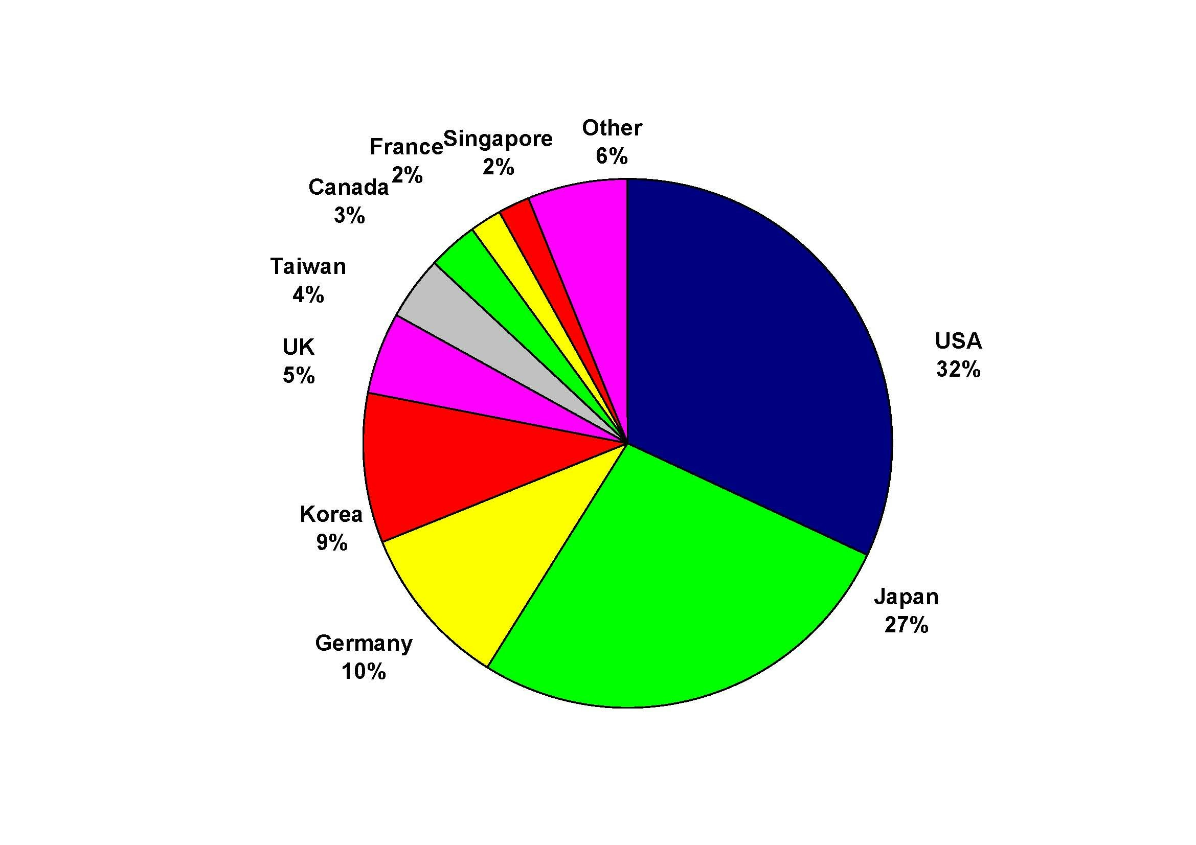
| 6.3. | Global electronics industry by application |
| 6.3. | Sales of printed and potentially printed transistors and memory by application in 2016 |
| 6.4. | Sales of printed and potentially printed transistors and memory by application in 2021 |
| 6.4. | End user markets relevant to printed electronics |
| 6.4. | Size of relevant markets that are impacted |
| 6.5. | Potential for non-RFID electronic labels |
| 6.5. | Global semiconductor shipments monthly and three month average 1983 to 2005 |
| 6.5. | Potential, in billions yearly, for global sales of RFID labels and circuits printed directly onto products or packaging. Item level is shown in red. These are examples. |
| 6.6. | Market for printed and potentially printed electronic devices by chemistry of key element 2011-2021 in billions of dollars |
| 6.6. | Statistics for electronic labels and their potential locations |
| 6.6. | Potential for RFID labels 2011-2021 |
| 6.7. | Market for RFID |
| 6.7. | Number (in millions) of passive tags by application 2011-2021 |
| 6.7. | Printed electronics materials and other elements of device income 2011-2021 |
| 6.7.2. | Ultimate potential for highest volume RFID |
| 6.7.3. | Penetration of chipless RFID |
| 6.8. | Impact on silicon |
| 6.8. | Current options and challenges for backplane TFTs |
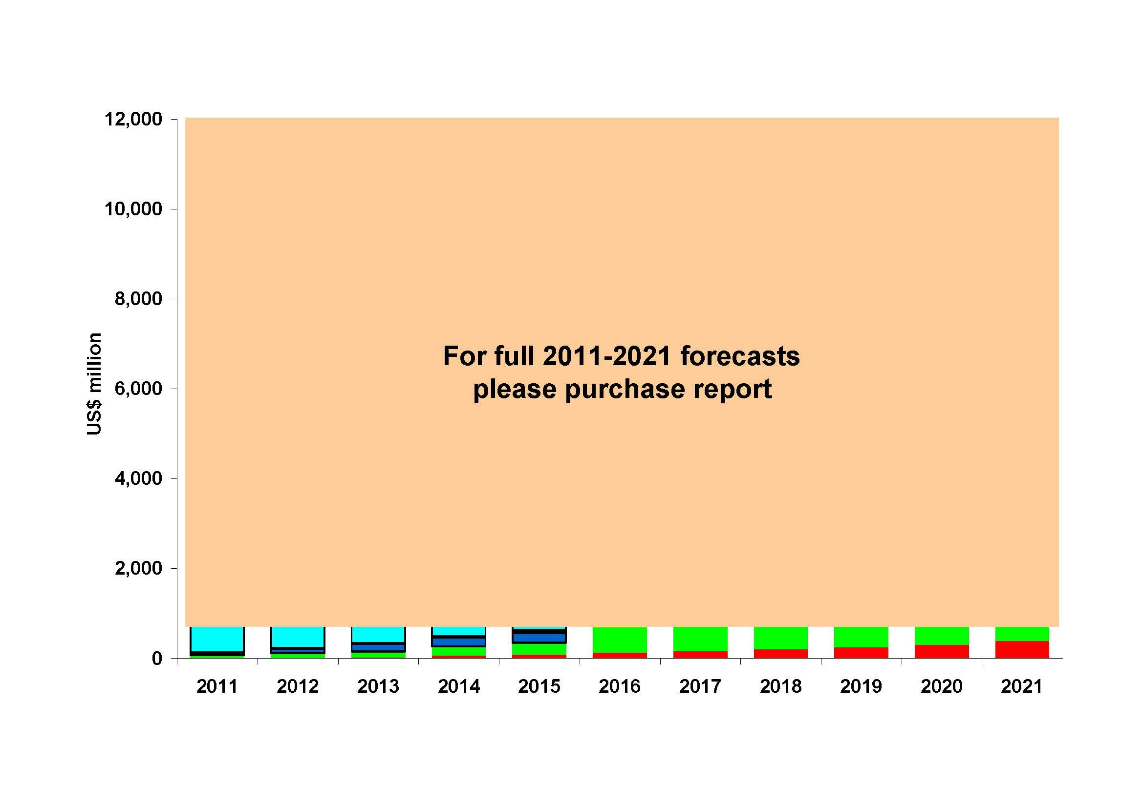
| 6.8. | Value of passive tags by application 2011-2021 (US Dollar Millions) |
| 6.9. | Choices of digital chipless RFID technologies |
| 6.9. | Forecasts for materials |
| 6.10. | Backplane transistor arrays hold up AMOLED market penetration |
| 6.10. | Chipless versus Chip RFID, in numbers of units (billions) 2011-2021 (includes passive and active RFID) |
| 6.11. | Market size of a variety of chipless solutions, US$ millions |
| 6.11. | Impediments to the commercialisation of printed transistors and memory |
| 6.12. | Scope for printed TFTCs to create new markets or replace silicon chips |
| 6.13. | Market for printed and potentially printed electronic devices 2011-2021 in billions of dollars |
| 6.14. | Printed electronics materials and other elements of device income 2011-2021 in billions of dollars |
| 7. | COMPARISON OF ORGANISATIONS INVOLVED IN TFTCS AND THEIR MATERIALS |
| 7.1. | Semiconductor, process, geometry, targets, challenges and objectives for 80 organisations in printed and thin film transistors and/ or memory |
| 7.1. | Objectives and challenges of 80 organisations developing printed and potentially printed transistor and/ or memory circuits and/or their materials |
| 7.1. | Fujitsu "electronic paper" display |
| 7.2. | Researchers and users play major roles with active logistic support from JST |
| 7.2. | Objectives and challenges of 23 organizations developing inks and their materials for printed and potentially printed transistors and memory |
| 7.2. | Profiles of 45 organisations in printed and thin film transistors and/ or memory |
| 7.2.1. | ACREO |
| 7.2.2. | AU Optoelectronics |
| 7.2.3. | BASF |
| 7.2.4. | Canon |
| 7.2.5. | CEA Liten |
| 7.2.6. | DaiNippon Printing |
| 7.2.7. | Dow Chemical |
| 7.2.8. | Ecole Superiure des Mines Saint Etienne |
| 7.2.9. | ETRI (Electronics and Telecommunications Research Institute) |
| 7.2.10. | Fraunhofer Institute for Photonic Microsystems |
| 7.2.11. | Fraunhofer Institute for Reliability and Microintegration |
| 7.2.12. | Fujitsu |
| 7.2.13. | Heraeus (formerly H.C.Starck) |
| 7.2.14. | Hewlett Packard |
| 7.2.15. | Hitachi |
| 7.2.16. | Impika |
| 7.2.17. | Industrial Technology Research Institute |
| 7.2.18. | Institute of Microelectronics |
| 7.2.19. | International University of Bremen |
| 7.2.20. | Japan Science and Technology Agency |
| 7.2.21. | Korea Electronics Technology Institute |
| 7.2.22. | Korea Institute of Science and Technology |
| 7.2.23. | Kovio |
| 7.2.24. | Kyung Hee University |
| 7.2.25. | Matsushita |
| 7.2.26. | Merck Chemicals |
| 7.2.27. | NHK |
| 7.2.28. | Oregon State University |
| 7.2.29. | Palo Alto Research Center |
| 7.2.30. | Paru |
| 7.2.31. | Plastic Logic |
| 7.2.32. | Poly IC |
| 7.2.33. | PragmatIC Printing (formerly ePrint) |
| 7.2.34. | Samsung Advanced Institute of Technology SAIT |
| 7.2.35. | Semiconductor Energy Laboratory |
| 7.2.36. | Sony |
| 7.2.37. | Sunchon National University |
| 7.2.38. | Thin Film Electronics |
| 7.2.39. | Tohoku University |
| 7.2.40. | Tokyo Institute of Technology |
| 7.2.41. | Toppan Printing |
| 7.2.42. | University of California Los Angeles |
| 7.2.43. | University of Cambridge |
| 7.2.44. | University of Tokyo |
| 7.2.45. | Xerox |
| 7.3. | 42 organisations that developing TFTCs and their materials and their priorities for products to be sold |
| 7.3. | High Mobility OTFT |
| 7.4. | Summary and Conclusion |
| 7.5. | PARC have developed innovative displays |
| 7.6. | Materials and devices. Fully printed RFID tag in development. |
| 7.7. | Fully printed EAS (anti theft) tag shown on website. |
| 7.8. | Prototype HF tag and reader |
| 7.9. | Left is diode logic OR gate and the right is a bridge rectifier |
| 7.10. | Micrograph of an SSD array and the 110 GHz microwave measurement setup |
| 7.11. | Samsung OLED display |
| 7.12. | A circuit by Associate Professor Zhenan Bao. |
| APPENDIX 1: IDTECHEX PUBLICATIONS AND CONSULTANCY | |
| TABLES | |
| FIGURES |

レポート概要
| ページ | 302 |
|---|---|
| Tables | 38 |
| 図 | 110 |
| フォーキャスト | 2021 |
Customer Testimonial
