| 1. | EXECUTIVE SUMMARY |
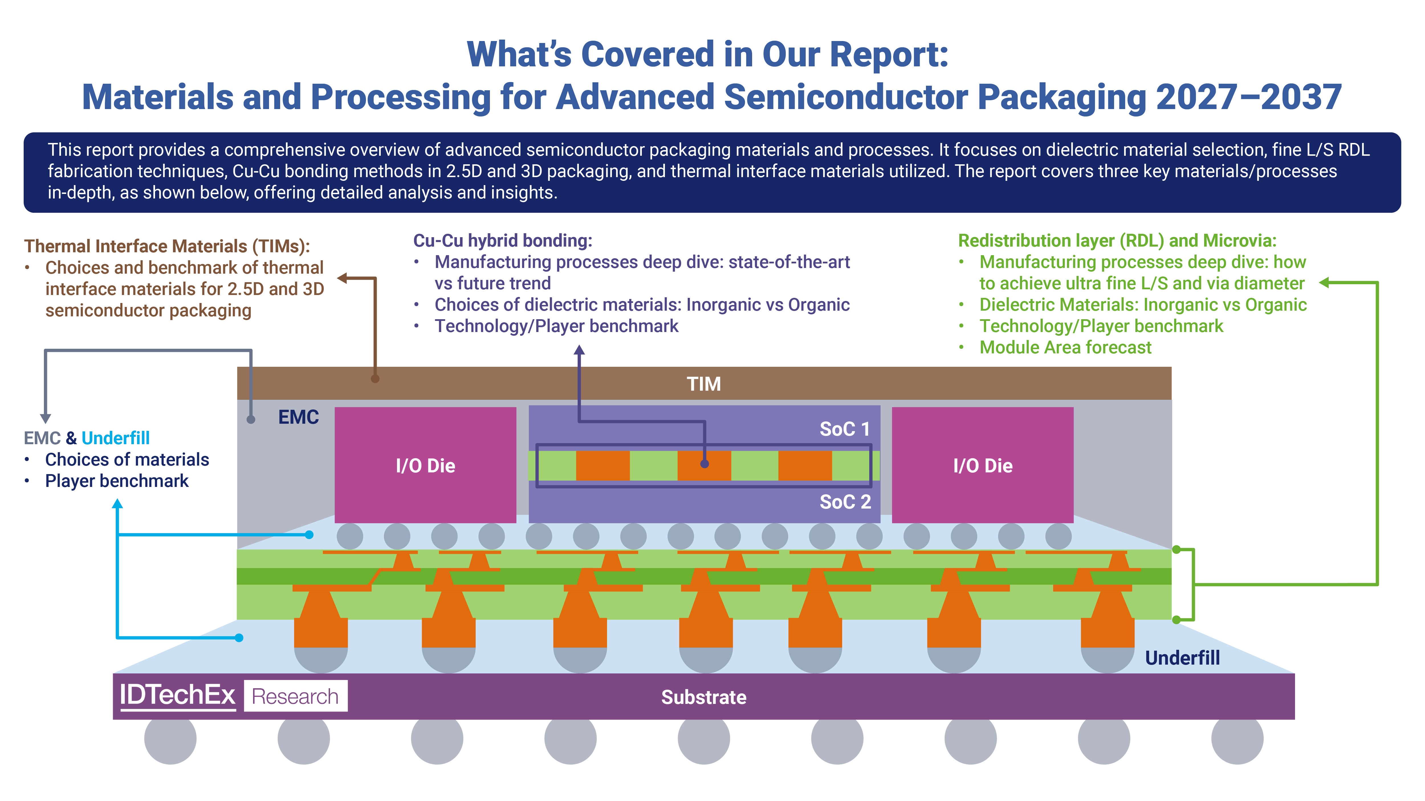
| 1.1. | Report scope |
| 1.2. | Evolution roadmap of semiconductor packaging |
| 1.3. | Overview of interconnection technique in semiconductor packaging |
| 1.4. | Development trend for 2.5D packaging |
| 1.5. | Key factors to consider when choosing material for electronic interconnects |
| 1.6. | Benchmark of materials for interposer |
| 1.7. | Key parameters for organic RDL materials for next generation 2.5D fan-out packaging |
| 1.8. | Benchmark of organic dielectrics for RDL |
| 1.9. | Benchmark of RDL formation technology |
| 1.10. | Benchmark of RDL formation technology (cont.) |
| 1.11. | Overview of via diameter range by different microvia creation technology (1) |
| 1.12. | Overview of key processes for glass core substrate |
| 1.13. | Comparison of different TGV formation processes |
| 1.14. | Comparison of TGV metallization processes |
| 1.15. | Supply chain overview for glass panel packaging |
| 1.16. | Benchmarking TGV capabilities across players |
| 1.17. | Future outlook for glass panel packaging |
| 1.18. | Evolution of bumping technologies |
| 1.19. | Three ways of Cu-Cu hybrid bonding |
| 1.20. | Benchmark: W2W vs direct D2W |
| 1.21. | Benchmark: W2W vs direct D2W |
| 1.22. | Overview of manufacturing factors impacting hybrid bonding quality |
| 1.23. | Overview of surface preparation steps for D2W bonding |
| 1.24. | Three key steps for room-temperature copper hybrid bonding |
| 1.25. | Key factors in hybrid bonding that are impacted by the choice of dielectric material |
| 1.26. | Inorganic dielectric vs organic dielectric: A quick overview |
| 1.27. | Technology benchmark of different dielectric materials for Cu-Cu hybrid bonding |
| 1.28. | TIM1 considerations |
| 1.29. | Potential TIM1 options in the future |
| 1.30. | Forecast: Organic dielectric advanced semiconductor packaging module area (Unit and mm2) - 1 |
| 1.31. | Forecast: Organic dielectric advanced semiconductor packaging module area (Unit and mm2) - 2 |
| 1.32. | Forecast: Advanced semiconductor packaging glass module area (Unit and mm2) - 2 |
| 1.33. | Access more with an IDTechEx subscription |
| 2. | INTRODUCTION TO ADVANCED SEMICONDUCTOR PACKAGING |
| 2.1. | Evolution roadmap of semiconductor packaging |
| 2.2. | Semiconductor packaging - an overview of technology |
| 2.3. | Advanced packaging 2.5D & 3D |
| 2.4. | Interposer technology |
| 2.5. | Evolution of bumping technologies |
| 2.6. | Bumpless Cu-Cu hybrid bonding |
| 2.7. | Advanced semiconductor packaging technologies - our scope |
| 2.8. | Key markets for advanced semiconductor packaging |
| 2.9. | Advanced Semiconductor Packaging - Ecosystem |
| 2.10. | Business value chain in the IC industry |
| 2.11. | Ecosystem/Business model in the IC industry |
| 2.12. | Role and advantages of players in advanced semiconductor packaging market |
| 2.13. | Players in advanced semiconductor packaging and their solutions |
| 2.14. | An overview of chip supply chain |
| 3. | ADVANCED SEMICONDUCTOR PACKAGING: PERFORMANCE EVALUATION, AND ITS LINK TO FABRICATION PROCESSES AND MATERIALS |
| 3.1.1. | Key factors impacting advanced semiconductor packaging performance |
| 3.1.2. | Primary considerations for advanced packaging |
| 3.1.3. | The key metrics that impact advanced semiconductor packaging performance: Bandwidth |
| 3.1.4. | The definition of IO density |
| 3.1.5. | IO density calculation |
| 3.1.6. | Routes to increase I/O density |
| 3.1.7. | The key metrics that impact advanced semiconductor packaging performance: Power efficiency |
| 3.2. | 2.5D packaging process flow know-how |
| 3.2.1. | 2.5D packaging - high density fan-out packaging |
| 3.2.2. | Two types of fan-out: Wafer level |
| 3.2.3. | Two types of fan-out: Panel level |
| 3.2.4. | Fan-out packaging process overview |
| 3.2.5. | Fan-out Chip-first process flow |
| 3.2.6. | Fan-out chip-last process flow |
| 3.2.7. | High level process concepts on panel |
| 3.2.8. | FOPLP process approaches |
| 3.2.9. | Key technical challenges for FOPLP |
| 3.2.10. | Overview of challenges for FOPLP |
| 3.2.11. | Differences between FOPLP and FOWLP - 1 |
| 3.2.12. | Differences between FOPLP and FOWLP - 2 |
| 3.2.13. | Key trends in fan-out packaging |
| 3.2.14. | Wafer level fan-out chip last RDL formation - development trend |
| 3.2.15. | Challenges in future fan-out process |
| 3.2.16. | 2.5D packaging that involves Si as electronic interconnect |
| 3.2.17. | Through-Si-Via (TSV) process flow |
| 3.2.18. | Dual damascene process flow (for inorganic RDL fabrication) |
| 3.2.19. | Process flow for Si interposer on package substrate |
| 3.2.20. | Glass core as interposer for advanced semiconductor packaging |
| 3.2.21. | Glass core (interposer) package - process flow |
| 3.2.22. | Fan out process flows from key companies |
| 3.2.23. | SPIL FOEB technology process flow |
| 3.2.24. | ASE FOCoS process flow (1) |
| 3.2.25. | Flip chip on FOWLP - Process flow |
| 3.2.26. | Samsung's FOWLP device structure |
| 3.3. | Redistribution layer (RDL) & Microvia - Materials |
| 3.3.1. | Redistribution Layer (RDL) |
| 3.3.2. | Key factors to consider when choosing material for electronic interconnects |
| 3.3.3. | Dielectric thickness of RDL |
| 3.3.4. | Electronic interconnects: SiO2 vs Organic dielectric |
| 3.3.5. | Limitations of SiO2 in 2.5D packaging |
| 3.3.6. | Electrical characteristics vs different RDL solution - Amkor's perspective |
| 3.3.7. | Replace inorganic dielectric with organic polymers? |
| 3.3.8. | Importance of low-loss RDL materials for different packaging technologies |
| 3.3.9. | Key parameters for organic RDL materials for next generation 2.5D fan-out packaging |
| 3.3.10. | Benchmark of organic dielectrics for RDL |
| 3.3.11. | Benchmark of material properties used in packaging |
| 3.3.12. | Dielectric challenges in fan-out applications - 1 |
| 3.3.13. | Dielectric challenges in fan-out applications - 2 |
| 3.3.14. | Industry players of organic RDL |
| 3.3.15. | RDL-dielectric suppliers: Toray's polyimide materials |
| 3.3.16. | Toray's solution for advanced semiconductor packaging |
| 3.3.17. | Low Dk and Low Df materials for RF devices - solution from Toray |
| 3.3.18. | RDL-dielectric suppliers: HD Microsystems |
| 3.3.19. | Low-curing temp. RDL from HD Microsystem |
| 3.3.20. | RDL-dielectric suppliers: DuPont's Arylalkyl polymers (1) |
| 3.3.21. | RDL-dielectric suppliers: DuPont's PID dryfilm |
| 3.3.22. | RDL-dielectric suppliers: DuPont's InterVia |
| 3.3.23. | RDL-dielectric suppliers: Taiyo Ink's epoxy-based RDL |
| 3.3.24. | RDL-dielectric suppliers: Ajinomoto's nanofiller ABF |
| 3.3.25. | RDL-dielectric supplier: Showa Denko |
| 3.3.26. | Low-loss RDL materials for mmWave: TSMC's InFO AiP |
| 3.3.27. | Comparison of polymer dielectric materials in current high performance packages |
| 3.3.28. | Overcoming Limitations of Si interposers with Glass |
| 3.3.29. | Glass vs molding compound |
| 3.3.30. | Benchmark of materials for interposer |
| 3.3.31. | Interposer material supplier landscape |
| 3.4. | Redistribution layer (RDL) & Microvia - Fabrication Processes |
| 3.4.1. | Overview of RDL fabrication technology |
| 3.4.2. | Semi-Additive Process (SAP) for RDL formation (organic dielectric) |
| 3.4.3. | Dual damascene process for RDL formation (organic dielectric) |
| 3.4.4. | Benchmark of RDL formation technology |
| 3.4.5. | Benchmark of RDL formation technology (cont.) |
| 3.4.6. | Overview of RDL L/S range by different RDL formation technology (1) |
| 3.4.7. | Overview of microvia creation technology |
| 3.4.8. | Fine scale microvia creation technology - technology trend |
| 3.4.9. | Overview of via diameter range by different microvia creation technology (1) |
| 3.4.10. | Overview of via diameter range by different microvia creation technology (2) |
| 3.4.11. | Overview of lithography challenges in high density RDL packaging |
| 3.4.12. | Bottlenecks for <2/2 µm L/S RDL scaling |
| 3.4.13. | Two key process considerations for below 2/2 µm L/S organic RDL |
| 3.4.14. | Cu dual damascene process for organic RDL formation - TSMC |
| 3.4.15. | Embedded Cu trace process - TSMC's high density fan-out package |
| 3.4.16. | How RDL affects transmission line loss? |
| 3.4.17. | Embedded trace RDL (ETR) process by Amkor (S-SWIFT package) |
| 3.4.18. | Embedded trace RDL (ETR) process for RDL formation - 1 |
| 3.4.19. | Embedded trace RDL (ETR) process for RDL formation - 2 |
| 3.4.20. | Summary: Organic RDL technology development trend - 1 |
| 3.4.21. | Summary: Organic RDL technology development trend - 2 |
| 3.4.22. | Temporary bonding and debonding |
| 3.4.23. | Mitsui Mining and Smelting Co. Ltd. Solution (1) |
| 3.4.24. | Mitsui Mining and Smelting Co. Ltd. Solution (2) |
| 3.4.25. | Mitsui Mining and Smelting Co. Ltd. Solution (3) |
| 3.5. | Epoxy molded compounds (EMC) and mold under fill (MUF) |
| 3.5.1. | What are EMC and MUFs? |
| 3.5.2. | Epoxy Molding Compound (EMC) |
| 3.5.3. | Key parameters for EMCs and EMC fillers |
| 3.5.4. | Experimental and commercial EMC products with low dielectric constant |
| 3.5.5. | Epoxy resin: Parameters of different resins and hardener systems |
| 3.5.6. | Supply chain for EMC materials |
| 3.5.7. | EMC innovation trends for high frequency applications |
| 3.5.8. | EMC for warpage management |
| 3.5.9. | Fillers for EMC |
| 3.5.10. | High warpage control EMC for FO-WLP |
| 3.5.11. | Possible solutions for warpage and die shift |
| 3.5.12. | EMC suppliers: Sumitomo Bakelite |
| 3.5.13. | EMC suppliers: Sumitomo Bakelite |
| 3.5.14. | EMC suppliers: Kyocera's EMCs for semiconductors |
| 3.5.15. | EMC suppliers: Samsung SDI |
| 3.5.16. | EMC suppliers: Showa Denko |
| 3.5.17. | EMC suppliers: Showa Denko's sulfur-free EMC |
| 3.5.18. | EMC suppliers: KCC Corporation |
| 3.5.19. | Molded underfill (MUF) |
| 3.5.20. | Liquid molding compound (LMC) for compression molding |
| 3.5.21. | Thermal challenges and materials solutions for vertical power delivery in advanced semiconductor packages (Henkel) |
| 3.5.22. | High-thermal Liquid Compression Molding (LCM) materials |
| 3.5.23. | High-thermal Capillary Underfill (CUF) strategy |
| 3.6. | Glass Panel-Based Packaging - Overview, Materials, and Processing |
| 3.6.1. | Glass substrates: Overcoming cost and warpage barriers in current system |
| 3.6.2. | Definition of glass core substrate/glass interposer |
| 3.6.3. | Glass Substrate Manufacturing |
| 3.6.4. | Overview of key processes for glass core substrate |
| 3.6.5. | Glass core substrate: Core layer fabrication |
| 3.6.6. | Glass core substrate: Build-up layer fabrication |
| 3.6.7. | Example: Glass core as interposer for advanced semiconductor packaging |
| 3.6.8. | Example: Glass interposer package process flow from Georgia Tech |
| 3.6.9. | Example: 3D Glass Panel Embedding (GPE) package |
| 3.6.10. | Example: 3D Glass Panel Embedding (GPE) package process flow |
| 3.6.11. | Achieving 2/2 um L/S on glass substrate |
| 3.6.12. | RDL dielectrics on glass substrate |
| 3.6.13. | Through Glass Via Formation |
| 3.6.14. | Overview of TGV formation methods |
| 3.6.15. | Comparison of different TGV formation processes |
| 3.6.16. | Mechanical and high-power laser drilling |
| 3.6.17. | Laser-induced modification and advanced wet etching (LIDE) |
| 3.6.18. | Photosensitive glass and wet etching |
| 3.6.19. | Which TGV process is best suited for advanced packaging? - 1 |
| 3.6.20. | Which TGV process is best suited for advanced packaging? - 2 |
| 3.6.21. | Laser-induced deep etching (LIDE) from LPKF |
| 3.6.22. | LMCE from BSP |
| 3.6.23. | Philoptics' TGV technology |
| 3.6.24. | Through Glass Via (TGV) Metallization |
| 3.6.25. | TGV metallization processes |
| 3.6.26. | Two-step process |
| 3.6.27. | Seed layer deposition in TGV metallization |
| 3.6.28. | Factors for alternative TGV metallization process |
| 3.6.29. | Comparison of TGV metallization processes |
| 3.6.30. | Players Development Status and Roadmap |
| 3.6.31. | Supply chain overview for glass panel packaging |
| 3.6.32. | Intel glass packaging roadmap |
| 3.6.33. | Intel's recent demonstration on glass packaging |
| 3.6.34. | TSMC CoPoS - Panel-Level Packaging Development |
| 3.6.35. | TSMC's CoPoS equipment supply chain (initial vendor list) |
| 3.6.36. | Samsung Electro-Mechanics glass packaging roadmap |
| 3.6.37. | Nippon Electric Glass Co., Ltd. (NEG) |
| 3.6.38. | Absolics glass packaging roadmap |
| 3.6.39. | Samtec |
| 3.6.40. | Dai Nippon Printing (DNP) |
| 3.6.41. | Dai Nippon Printing (DNP)'s recent demonstration on glass packaging |
| 3.6.42. | Toppan |
| 3.6.43. | Toppan's recent demonstration on glass packaging |
| 3.6.44. | LG Innotek |
| 3.6.45. | Unimicron |
| 3.6.46. | FZX |
| 3.6.47. | Plan Optik AG |
| 3.6.48. | Plan Optik AG's technology |
| 3.6.49. | KCC |
| 3.6.50. | Display companies entering glass semiconductor packaging - 1 |
| 3.6.51. | Display companies entering glass semiconductor packaging - key players |
| 3.6.52. | Panel level processing development (Lam) |
| 3.6.53. | Lam panel roadmap: Three core process pillars |
| 3.6.54. | Lam's panel processing product portfolio |
| 3.6.55. | Glass-Based Packaging Summary: Progress, Challenges, and Outlook |
| 3.6.56. | Overview of manufacturing challenges and key development directions: Manufacturing environment |
| 3.6.57. | Overview of manufacturing challenges: Glass cracking and mechanical reliability |
| 3.6.58. | Key development directions: Glass cracking and mechanical reliability |
| 3.6.59. | Overview of manufacturing challenges: TGV process control and yield |
| 3.6.60. | Key development directions: TGV process control and yield |
| 3.6.61. | Key TGV technology development directions - 1 |
| 3.6.62. | Key TGV technology development directions - 2 |
| 3.6.63. | Benchmarking TGV capabilities across players |
| 3.6.64. | Fine-line RDL |
| 3.6.65. | Glass substrate adoption innovations in semiconductor packaging |
| 3.6.66. | Glass innovation efforts |
| 3.6.67. | Expected substrate sizes expected to become future standards |
| 3.6.68. | Future outlook for glass panel packaging |
| 4. | CU-CU HYBRID BONDING TECHNOLOGY FOR 3D DIE STACKING |
| 4.1.1. | Evolution of bumping technologies |
| 4.1.2. | Challenges in conventional bumping |
| 4.1.3. | Micro bumps (µ bumps) vs bumpless Cu-Cu hybrid bonding |
| 4.1.4. | Bonding pitch size needs to scale with TSV development |
| 4.1.5. | Performance benchmark of devices based on micro bumps vs Cu-Cu bumpless hybrid bonding - 1 |
| 4.1.6. | Overview of applications that make use of 3D Cu-Cu hybrid bonding |
| 4.1.7. | Key concepts about hybrid bonding |
| 4.2. | Cu-Cu hybrid bonding - manufacturing processes and bonding tools |
| 4.2.1. | Cu-Cu hybrid bonding processes breakdown |
| 4.2.2. | Overview of manufacturing factors impacting hybrid bonding quality |
| 4.2.3. | Three ways of Cu-Cu hybrid bonding |
| 4.2.4. | Generic W2W process flow |
| 4.2.5. | Generic D2W process flow |
| 4.2.6. | W2W hybrid bonding - process parameter |
| 4.2.7. | Generic collective D2W process |
| 4.2.8. | Overview of process comparison direct D2W vs W2W vs Collective D2W |
| 4.2.9. | Benchmark: W2W vs direct D2W |
| 4.2.10. | Benchmark: W2W vs direct D2W |
| 4.2.11. | Benchmark: Collective D2W or direct D2W |
| 4.2.12. | Process flow for memory stacking using D2W hybrid bonding - 1 |
| 4.2.13. | Process flow for memory stacking using D2W hybrid bonding - 2 |
| 4.2.14. | Overview of surface preparation steps for D2W bonding |
| 4.2.15. | D2W know-how: Surface treatment |
| 4.2.16. | D2W know-how: Contamination management |
| 4.2.17. | D2W know-how: Die placement and tool consideration |
| 4.2.18. | Annealing temperature for hybrid bonding |
| 4.2.19. | Growing demand for low/room-temperature copper hybrid bonding |
| 4.2.20. | Low/room-temperature copper hybrid bonding - mechanism |
| 4.2.21. | Three key steps for room-temperature copper hybrid bonding |
| 4.2.22. | Methods to enable low-temperature Cu-Cu bonding - 1 |
| 4.2.23. | Methods to enable low-temperature Cu-Cu bonding - 2 |
| 4.2.24. | Case studies: Approaches to lower annealing temperature |
| 4.2.25. | Room temperature hybrid bonding - CEA-Leti |
| 4.2.26. | Case studies: Low-temperature hybrid bonding enabled by copper microstructure engineering (MKS Atotek) - 1 |
| 4.2.27. | Case studies: Low-temperature hybrid bonding enabled by copper microstructure engineering (MKS Atotek) - 2 |
| 4.2.28. | Hybrid bonding tool development |
| 4.2.29. | Tool suppliers in 3DIC hybrid bonding |
| 4.2.30. | Hybrid bonding process options - available performance of current bonding tool |
| 4.2.31. | State-of-the-art W2W and D2E bonder from EVG |
| 4.2.32. | State-of-the-art D2W bonder from Besi |
| 4.2.33. | Besi's portfolio on multiple 3D technologies |
| 4.2.34. | Applied materials portfolio in advanced semiconductor packaging |
| 4.2.35. | Kinex - a fully integrated die-to-wafer hybrid bonding system |
| 4.2.36. | Integrated D2W hybrid bonding process flow |
| 4.2.37. | Benefits of integrated hybrid bonding tools |
| 4.2.38. | Known users for Kinex |
| 4.2.39. | W2W/D2W bonder from SUSS |
| 4.2.40. | 3D bonding equipment portfolios from TEL |
| 4.2.41. | 3D SoIC manufacturing processes deep dive |
| 4.2.42. | 3D SoIC process flow deep dive - 1 |
| 4.2.43. | 3D SoIC process flow deep dive - 2 |
| 4.2.44. | 3D SoIC process flow deep dive - 3 |
| 4.2.45. | 3D SoIC process flow deep dive - 4 |
| 4.2.46. | Application examples of 3D SoIC packages |
| 4.2.47. | Key applications of 3D SoIC packages |
| 4.2.48. | 3D SoIC process - a quick overview |
| 4.2.49. | Challenges in Cu-Cu hybrid bonding manufacturing process |
| 4.3. | Cu-Cu hybrid bonding -the choice of materials |
| 4.3.1. | Choices of dielectric materials for hybrid bonding |
| 4.3.2. | Key factors in hybrid bonding that are impacted by the choice of dielectric material |
| 4.3.3. | Challenges in using inorganic dielectric materials |
| 4.3.4. | Benefits of organic dielectric materials |
| 4.3.5. | Challenges of using organic dielectric materials |
| 4.3.6. | Inorganic dielectric vs organic dielectric: a quick overview |
| 4.3.7. | Technology benchmark of different dielectric materials for Cu-Cu hybrid bonding |
| 4.3.8. | Polymer-based dielectric hybrid bonding |
| 4.4. | Cu-Cu hybrid bonding based on organic dielectric - case studies |
| 4.4.1. | HD Microsystem 's polyimide solution for hybrid bonding - 1 |
| 4.4.2. | HD Microsystem 's polyimide solution for hybrid bonding - 2 |
| 4.4.3. | Showa Denko Copper/Polyimide hybrid bonding - 1 |
| 4.4.4. | Showa Denko Copper/Polyimide hybrid bonding - 2 |
| 4.4.5. | Cu/Polymer hybrid bonding simulation results from IME |
| 4.4.6. | Polyimide/Cu hybrid bonding materials characterization from Applied Materials & IME |
| 4.4.7. | Brewer Science - photosensitive permanent bonding materials for polymer/Cu hybrid bonding - 1 |
| 4.4.8. | Brewer Science - photosensitive permanent bonding materials for polymer/Cu hybrid bonding - 2 |
| 4.4.9. | Key summary of polymer dielectric for hybrid bonding research |
| 4.4.10. | Comparison of polymer case studies for hybrid bonding benchmarking |
| 4.4.11. | Keys to select the right polymer for Cu-Cu hybrid bonding |
| 4.4.12. | List of inorganic fillers for CTE improvement in polymers |
| 4.4.13. | List of inorganic fillers for thermal conductivity improvement in polymers |
| 4.5. | Cu-Cu hybrid bonding based on inorganic dielectric |
| 4.5.1. | Samsung's Cu-Cu bonding |
| 4.5.2. | Cu-Cu hybrid bonding - Mitsubishi Heavy Industries Machine Tool |
| 4.5.3. | Improved Cu-Cu hybrid bonding through Cu enlargement - a study from Tohoku/T-Micro/JCU |
| 4.5.4. | 1 µm pitch Cu-Cu hybrid bonding base on SiCN - a study from imec |
| 4.5.5. | Self-assembly for hybrid bonding - A study from CEA-Leti and Intel |
| 4.5.6. | SiO2 C2W hybrid bonding from IME |
| 4.5.7. | Die stacking from Xperi (Adeia) |
| 4.5.8. | XPERI(ADEIA) license map |
| 4.5.9. | TSMC hybrid bonding technology for AMD CPU |
| 4.5.10. | Stacking DRAMs using hybrid bonding - a study from SK Hynix |
| 4.5.11. | Sony's hybrid bonding - recent development |
| 4.5.12. | Key process know-how for inorganic dielectric Cu-Cu hybrid bonding |
| 4.5.13. | Cu/Sn-Cu/Sn hybrid bonding |
| 5. | THERMAL INTERFACE MATERIALS FOR ADVANCED SEMICONDUCTOR PACKAGING |
| 5.1. | Thermal characteristics and challenges of 2.5D/3D packages |
| 5.2. | Thermal benefits of advanced semiconductor packaging in HPC chips |
| 5.3. | Die-attach for CPUs, GPUs and memory modules |
| 5.4. | Die attach materials comparison |
| 5.5. | Thermal interface material inside the packaging - TIM1 |
| 5.6. | Where are TIM1 used |
| 5.7. | TIM1 considerations |
| 5.8. | Potential TIM1 options in the future |
| 5.9. | Indium foil TIM1 - issues with multiple reflow process |
| 5.10. | Traditional and mature product - Shin-Estu X-23 series for BGA |
| 5.11. | Thermal gel - Shin-Etsu MicroSi |
| 5.12. | Silver-filled thermal grease - potential solution for FCBGA |
| 5.13. | Graphene - proved uses as TIM1.5 and Resonac's Graphene has been used as TIM1 |
| 5.14. | Graphene - bare die + TIM1.5 most popular method with wrapping process |
| 5.15. | Liquid metal - TIM1 or TIM1.5 for 2.5D packaging |
| 5.16. | Challenges of liquid metals and solution of using solid/liquid approach from Indium Corp |
| 5.17. | Indium Corp - liquid metal |
| 5.18. | Yunnan Zhongxuan Liquid Metal Technology Co., Ltd. |
| 5.19. | Yunnan Zhongxuan - helping with establishing the industry standard of liquid metal |
| 5.20. | Liquid metals for servers - Nvidia 5090 |
| 5.21. | Thermally conductive sheet using vertical oriented graphite fillers as TIM1 |
| 5.22. | Resonac TIMs |
| 5.23. | Arieca - liquid metal embedded elastomer (LMEEs) |
| 5.24. | Arieca - LMEEs Test |
| 5.25. | Diamond as TIM0 to avoid hotspots - early research stage |
| 5.26. | Integrated Si Micro-Cooler with liquid metal and SiOx TIM |
| 5.27. | Chip and package level - CuNWs/PDMS based TIMs |
| 5.28. | Liquid CuNW infused nanostructured composite as TIM (1/2) |
| 5.29. | Liquid CuNW infused nanostructured composite as TIM (2/2) |
| 6. | MARKET FORECAST |
| 6.1. | Forecast methodology |
| 6.2. | Forecast: Organic dielectric advanced semiconductor packaging module area (unit and mm2) - 1 |
| 6.3. | Forecast: Organic Dielectric Advanced Semiconductor Packaging Module Area (Unit and mm2) - 2 |
| 6.4. | Forecast: Advanced semiconductor packaging glass module area (unit and mm2) - 2 |
| 7. | COMPANY PROFILES |
| 7.1. | Access to company profiles on the IDTechEx portal |

 Sample pages
